Last time we have tried to do single conversion of one channel. We were waiting for result in a loop which isn’t effective way of using processor resources. It is better to trigger conversion and wait for conversion complete interrupt. During this time processor can do other tasks rather than wait for ADC conversion complete. So this time we will go through another example where we will set up more than one channel and read ADC values within interrupt service routine.
Image may be NSFW.
Clik here to view.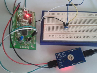
If we need to convert several channels continuously, we need to set up Sequence registers (ADC_SQRx). There are three sequence registers: ADC_SQR1, ADC_SQR2 and ADC_SQR3 where we can set up maximum 16 channels in any order. Conversion sequence starts with SQ1[4:0] settings in ADC_SQR3 register. Bits [4:0] hold the number of ADC channel.
Image may be NSFW.
Clik here to view.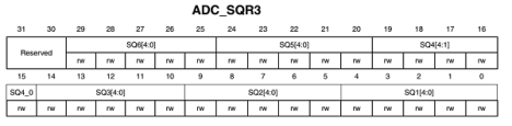
All 16 sequence channels can be set up same way through all SQR registers. Then in ADC_SQR1 register there are four bits marked L[3:0] where you can set the number how many times sequence reading will be repeated.
Another thing we will have to take care is to set up sample time for each channel. As we know each channel in sequence can be set for different conversion time. Sampling time for each channel can be set up in two registers: ADC_SMPR1 and ADC_AMPR2. There are three bits for each channel in sequence.
Image may be NSFW.
Clik here to view.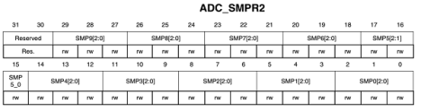
If you use standard peripheral library setting up is really easy.
Lets write an example where we will read first 8 ADC channels four times using scan mode. Then calculate average of each channel and then print results on terminal screen via UART. We will store ADC values by using DMA channel. Once all data is stored in memory an DMA transfer complete interrupt will be generated to trigger averaging and output. From STM32F100x datasheet we find that ADC pins are as alternate functions as follows:
ADC1_IN0 – PA0
ADC1_IN1 – PA1
ADC1_IN2 – PA2
ADC1_IN3 – PA3
ADC1_IN4 – PA4
ADC1_IN5 – PA5
ADC1_IN6 – PA6
ADC1_IN7 – PA7
ADC1_IN8 – PB0
ADC1_IN9 – PB1
ADC1_IN10 – PC0
ADC1_IN11 – PC1
ADC1_IN12 – PC2
ADC1_IN13 – PC3
ADC1_IN14 – PC4
ADC1_IN15 – PC5
For first eight channels we will need to set up pins A0 to A7 as analog inputs. Then we can set up ADC conversion mode. We need to set up Scan Conversion Mode to be able go through all channels selected in ADC1_SQRx registers. By using peripheral library this looks like:
ADC_InitStructure.ADC_ScanConvMode = ENABLE;
Then we must enable to enable continuous conversion mode as we want to cycle through channel list several times:
ADC_InitStructure.ADC_ContinuousConvMode = ENABLE;
Then we indicate nuber of channels to be converted in scan mode:
ADC_InitStructure.ADC_NbrOfChannel = 8;
Next thing is to indicate which channels and what order we need to convert. For this we set up each channel individually with commands:
ADC_RegularChannelConfig(ADC1, ADC_Channel_0, 1, ADC_SampleTime_41Cycles5);
ADC_RegularChannelConfig(ADC1, ADC_Channel_1, 2, ADC_SampleTime_41Cycles5);
ADC_RegularChannelConfig(ADC1, ADC_Channel_2, 3, ADC_SampleTime_41Cycles5);
ADC_RegularChannelConfig(ADC1, ADC_Channel_3, 4, ADC_SampleTime_41Cycles5);
ADC_RegularChannelConfig(ADC1, ADC_Channel_4, 5, ADC_SampleTime_41Cycles5);
ADC_RegularChannelConfig(ADC1, ADC_Channel_5, 6, ADC_SampleTime_41Cycles5);
ADC_RegularChannelConfig(ADC1, ADC_Channel_5, 7, ADC_SampleTime_41Cycles5);
ADC_RegularChannelConfig(ADC1, ADC_Channel_7, 8, ADC_SampleTime_41Cycles5);
I’ve chosen to go all 8 channels in the row from 0 to 7. But you can mess up the numbers as you like. The rest is to set up DMA where it copies ADC values to memory on each EOC event. After DMA copies predefined number of values it generates interrupt. Then we can manipulate data as we like. As in our example we simply average multiple instances.
This is a result on terminal screen.
Image may be NSFW.
Clik here to view.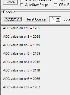
You can hook up a potentiometer or any other analog sensor to each channel to see its ADC value.
Here is the complete main source code if you would like to analyze or use fragments for your own purposes:
// Includes ------------------------------------------------------------------*/
#include "stm32f10x.h"
#include "usart.h"
#include <stdio.h>
#define ARRAYSIZE 8*4
#define ADC1_DR    ((uint32_t)0x4001244C)
volatile uint16_t ADC_values[ARRAYSIZE];
volatile uint32_t status = 0;

void ADCInit(void);
void DMAInit(void);
int main(void)
{
uint8_t index;
//initialize USART1
Usart1Init();
ADCInit();
DMAInit();

//Enable DMA1 Channel transfer
DMA_Cmd(DMA1_Channel1, ENABLE);
//Start ADC1 Software Conversion
ADC_SoftwareStartConvCmd(ADC1, ENABLE);
//wait for DMA complete
while (!status){};
ADC_SoftwareStartConvCmd(ADC1, DISABLE);
//print averages
/*for(index = 0; index<8; index++)
	{
	printf("ch%d = %d ",index, ADC_values[index]);
	}*/
for(index = 0; index<8; index++){
	printf("\r\n ADC value on ch%d = %d\r\n",
			index, (uint16_t)((ADC_values[index]+ADC_values[index+8]
					+ADC_values[index+16]+ADC_values[index+24])/4));
}

while (1)
  {
	//interrupts does the job
  }
}

void ADCInit(void){
	//--Enable ADC1 and GPIOA--
	RCC_APB2PeriphClockCmd(RCC_APB2Periph_ADC1 | RCC_APB2Periph_GPIOA, ENABLE);
	GPIO_InitTypeDef GPIO_InitStructure; //Variable used to setup the GPIO pins
	//==Configure ADC pins (PA0 -> Channel 0 to PA7 -> Channel 7) as analog inputs==
	GPIO_StructInit(&GPIO_InitStructure); // Reset init structure, if not it can cause issues...
	GPIO_InitStructure.GPIO_Pin = GPIO_Pin_0 | GPIO_Pin_1| GPIO_Pin_2| GPIO_Pin_3| GPIO_Pin_4| GPIO_Pin_5| GPIO_Pin_6| GPIO_Pin_7;
	GPIO_InitStructure.GPIO_Mode = GPIO_Mode_AIN;
	GPIO_Init(GPIOA, &GPIO_InitStructure);

	ADC_InitTypeDef ADC_InitStructure;
	//ADC1 configuration

	ADC_InitStructure.ADC_Mode = ADC_Mode_Independent;
	//We will convert multiple channels
	ADC_InitStructure.ADC_ScanConvMode = ENABLE;
	//select continuous conversion mode
	ADC_InitStructure.ADC_ContinuousConvMode = ENABLE;//!
	//select no external triggering
	ADC_InitStructure.ADC_ExternalTrigConv = ADC_ExternalTrigConv_None;
	//right 12-bit data alignment in ADC data register
	ADC_InitStructure.ADC_DataAlign = ADC_DataAlign_Right;
	//8 channels conversion
	ADC_InitStructure.ADC_NbrOfChannel = 8;
	//load structure values to control and status registers
	ADC_Init(ADC1, &ADC_InitStructure);
	//wake up temperature sensor
	//ADC_TempSensorVrefintCmd(ENABLE);
	//configure each channel
	ADC_RegularChannelConfig(ADC1, ADC_Channel_0, 1, ADC_SampleTime_41Cycles5);
	ADC_RegularChannelConfig(ADC1, ADC_Channel_1, 2, ADC_SampleTime_41Cycles5);
	ADC_RegularChannelConfig(ADC1, ADC_Channel_2, 3, ADC_SampleTime_41Cycles5);
	ADC_RegularChannelConfig(ADC1, ADC_Channel_3, 4, ADC_SampleTime_41Cycles5);
	ADC_RegularChannelConfig(ADC1, ADC_Channel_4, 5, ADC_SampleTime_41Cycles5);
	ADC_RegularChannelConfig(ADC1, ADC_Channel_5, 6, ADC_SampleTime_41Cycles5);
	ADC_RegularChannelConfig(ADC1, ADC_Channel_5, 7, ADC_SampleTime_41Cycles5);
	ADC_RegularChannelConfig(ADC1, ADC_Channel_7, 8, ADC_SampleTime_41Cycles5);
	//Enable ADC1
	ADC_Cmd(ADC1, ENABLE);
	//enable DMA for ADC
	ADC_DMACmd(ADC1, ENABLE);
	//Enable ADC1 reset calibration register
	ADC_ResetCalibration(ADC1);
	//Check the end of ADC1 reset calibration register
	while(ADC_GetResetCalibrationStatus(ADC1));
	//Start ADC1 calibration
	ADC_StartCalibration(ADC1);
	//Check the end of ADC1 calibration
	while(ADC_GetCalibrationStatus(ADC1));
}
void DMAInit(void){
	//enable DMA1 clock
	RCC_AHBPeriphClockCmd(RCC_AHBPeriph_DMA1, ENABLE);
	//create DMA structure
	DMA_InitTypeDef  DMA_InitStructure;
	//reset DMA1 channe1 to default values;
	DMA_DeInit(DMA1_Channel1);
	//channel will be used for memory to memory transfer
	DMA_InitStructure.DMA_M2M = DMA_M2M_Disable;
	//setting normal mode (non circular)
	DMA_InitStructure.DMA_Mode = DMA_Mode_Normal;
	//medium priority
	DMA_InitStructure.DMA_Priority = DMA_Priority_High;
	//source and destination data size word=32bit
	DMA_InitStructure.DMA_PeripheralDataSize = DMA_PeripheralDataSize_HalfWord;
	DMA_InitStructure.DMA_MemoryDataSize = DMA_MemoryDataSize_HalfWord;
	//automatic memory destination increment enable.
	DMA_InitStructure.DMA_MemoryInc = DMA_MemoryInc_Enable;
	//source address increment disable
	DMA_InitStructure.DMA_PeripheralInc = DMA_PeripheralInc_Disable;
	//Location assigned to peripheral register will be source
	DMA_InitStructure.DMA_DIR = DMA_DIR_PeripheralSRC;
	//chunk of data to be transfered
	DMA_InitStructure.DMA_BufferSize = ARRAYSIZE;
	//source and destination start addresses
	DMA_InitStructure.DMA_PeripheralBaseAddr = (uint32_t)ADC1_DR;
	DMA_InitStructure.DMA_MemoryBaseAddr = (uint32_t)ADC_values;
	//send values to DMA registers
	DMA_Init(DMA1_Channel1, &DMA_InitStructure);
	// Enable DMA1 Channel Transfer Complete interrupt
	DMA_ITConfig(DMA1_Channel1, DMA_IT_TC, ENABLE);
	DMA_Cmd(DMA1_Channel1, ENABLE); //Enable the DMA1 - Channel1
	NVIC_InitTypeDef NVIC_InitStructure;
	//Enable DMA1 channel IRQ Channel */
	NVIC_InitStructure.NVIC_IRQChannel = DMA1_Channel1_IRQn;
	NVIC_InitStructure.NVIC_IRQChannelPreemptionPriority = 0;
	NVIC_InitStructure.NVIC_IRQChannelSubPriority = 0;
	NVIC_InitStructure.NVIC_IRQChannelCmd = ENABLE;
	NVIC_Init(&NVIC_InitStructure);


}
Also you can download project files [STM32DiscoveryADC_DMAmultiple.zip] that compiles with Codebench GCC and Eclipse.